 Differential amplifier with classic long-tailed pairDifferential amplifier with classic long-tailed pair
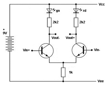
Slight
diffences in the base voltages of the transitors result in substantial
differences in the collector voltages. If Vin+ > Vin-, the collector
current through the left transtistor is greater than the collector
current through the right transtistor. Hence Vout+ >>
Vout-. Contrarily, if Vin+ < Vin- then Vout+ << Vout-.
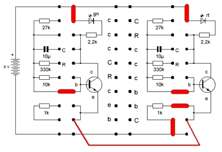
Experiments and Results
For the experiments extra wires, like the one that connects the emittors, are necessary. See the video.
Connect
the plus pole of a multimeter to the collector of the right transistor.
Connect the minus pole of the meter to the collector of the left
transistor. The collectors of the transistors form the output of the
differential amplifier. The bases form the input. With open bases the
transistors are not conducting, the LED's are off and the difference
between Vout+ and Vout- is close to zero, as shown on the multimeter.
Hold
a (wet) finger against the top left three pins of the connector of the
left circuit block. The base of the left transistor, being the positive
input of the differential amplifier, becomes positive. This results in
current flowing through the left transistor. The green LED comes on and
Vout- drops below Vout+. The output voltage of the differential
amplifier, as measured on the multimeter, rises to as much as + 4 to 5
Volts.
Hold a (wet) finger against the top left three pins of
the connector of the right circuit block. This gives the opposite
effect. The negative input of the differential amplifier becomes
positive. The red LED comes on and the output voltage measured on the
multimeter drops negative to as much as - 4 to 5 Volts.
Connect
the bases of both transistors to each other, using a wire between the
b's on the left and right connector. The output stays zero, as can be
expected of a differential amplifier. Connect another wire to one of
the b's on the middle connector. Touch this wire with your hand,
connect it to the positive battery terminal (Vcc), and connect it to
the negative battery terminal (Vee). In all this situations the output
should remain close to zero volts. This is indeed the case. There is so
called "common mode rejection". However temporary unbalance can occur,
which can be seen by flickering of the LED's.
Now remove the
connection between the bases and connect the 27k resistor of the left
block to Vcc. The green LED comes on and the output voltage measured on
the multimeter becomes 5.3 V. Only one transistor is conducting.
Connect the 27k resistor of the right block to +. The red LED comes on
too. The transistors are now both conducting at their maximum. The
output voltage becomes 0.0 V again.
Now connect the 10k
resistors of both the left and the right block to Vee, using wires. You
now have created voltage dividers for the Vb's of the transistors. They
are partly conducting now, being half way their caracteristics. The
output voltage as measured on the meter is close to zero volts,
but not perfectly as you would expect of an ideal differential
amplifier. This unbalance is due to an unbalance in the components,
especially in the gains of the transistors. You can demonstrate this by
warming up the transistors with your finger. Warming up one transistor
gives more balance. Warming up the other less balance.
Link to a video:
https://goo.gl/photos/B7VMJ28ftdnZPH2E9
See also:
Tony R. Kuphaldt - Operational Amplifiers - Excerpt